Building a GPU PC, Part 1: Understanding Modern DIY PC Architecture

Before building a PC, I want to start by learning about the PC architecture of today, as of 2023.
CPU, Motherboard, and Chipset
Chipset
A motherboard carries an important component called the "chipset," which manages communication between the various parts.
Each chipset supports a fixed set of CPUs, and you cannot install a CPU that the chipset does not support.
Conversely, from the CPU's point of view, the chipsets that can support a given CPU are limited.
A given CPU is not limited to a single chipset; multiple chipsets support it, differing in the level of features they implement.
Chipset, CPU, and CPU Socket Type
As explained above, chipsets and CPUs have a fixed correspondence, and the socket type used to seat the CPU on the motherboard also matches physically.
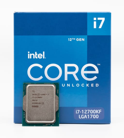
For example, the Z690 chipset supports the 12th-generation Intel Core i7 12700 CPU.
The socket type of the Intel Core i7 12700 is LGA 1700, and
naturally, motherboards with the Z690 chipset are designed to accept CPUs with the LGA 1700 socket type.
The chipsets for 12th-generation Core series CPUs are known as the Intel 600 series, and there are several of them, such as "Z690," "H670," "B660," and "H610." They differ in features, such as whether they support overclocking.
There are also Intel 700 series chipsets, such as "Z790," "H770," and "B760."
In fact, both the Intel 600 series and 700 series chipsets use the LGA1700 socket, so
both 12th-generation and 13th-generation Intel Core series CPUs can be seated in them. However, not every combination works, and some motherboards require a BIOS update, so you need to check compatibility for each motherboard.
Credit [Jacek Halicki] / Wikimedia Commons / CC-BY-SA-4.0
Northbridge and Southbridge
Today the CPU and the chipset each have their own division of roles, but in PCs of a generation ago there was a time when the roles were roughly split between a northbridge and a southbridge. To understand how roles are divided between the CPU and the chipset, let's take a brief look back at the history of PC architecture.
The northbridge referred to the component located at the top of the motherboard, and the southbridge to the one at the bottom. North is up and south is down, just as on an ordinary map.
(Java Swing also used north and south for layout positions, so this metaphor was probably fairly intuitive back in the day.)
The northbridge communicated directly with the CPU, RAM, and PCI Express devices (such as graphics cards). Because this part required high performance, its role was to connect to components that needed high-speed communication.
Today, however, the functions of the northbridge are in most cases integrated into the CPU, and it is the CPU, not the chipset, that handles this high-speed communication.
The southbridge communicates with I/O devices (USB, audio, serial devices, and so on), the BIOS, IDE, LAN cards, and the like. These are relatively slow components that do not require large volumes of data transfer.
Today, the role of the southbridge is mainly handled by the chipset.
So it is enough to remember the division of labor: high-speed communication is the CPU's job, and slower work such as I/O devices is the chipset's job.
PCI Express and "Lanes"
PCI Express is a slot and communication standard for connecting graphics cards and other expansion cards to the motherboard. This standard uses transmission paths called " lanes " to send and receive data.
A lane can be used on its own, but bundling multiple lanes together enables even faster communication. Bundling lanes in this way greatly improves data transfer efficiency and makes it possible to handle the large volumes of data transfer demanded by high-performance expansion cards. This is why PCI Express plays such an important role in modern computer systems.
Remember: PCI Express has transmission paths called lanes, and bundling multiple lanes makes it faster.
Lane Speed
The speed per lane is defined by the standard for each generation of PCI Express, as shown below.
- PCI Express can be abbreviated as PCIe
- PCI Express has generations (versions); PCI Express version 1.0 is sometimes abbreviated as gen1, PCI Express version 2.0 as gen2, and so on.
| Generation | Transfer rate (one direction) | |
|---|---|---|
| PCIe gen 1 | 2.5 gbits/s | 0.3125 gbytes/s |
| PCIe gen 2 | 5 gbits/s | 0.625 gbytes/s |
| PCIe gen 3 | 8 gbits/s | 1 gbytes/s |
| PCIe gen 4 | 16 gbits/s | 2 gbytes/s |
| PCIe gen 5 | 32 gbits/s | 4 gbytes/s |
As the table shows, with 5th-generation PCI Express, a single lane provides a transfer rate of 4 GByte/s.
The transfer rate doubles with each new generation of PCI Express.
Transfer Rates When Multiple Lanes Are Bundled
For example, a PCIe gen 5 transmission path with 16 lanes bundled together is written as PCIe gen5 x16.
This means it can transfer data at 64GB/s.
The number of bundled lanes and the corresponding transfer rates are summarized below.
x4 (bandwidth with 4 lanes)
| Generation | Transfer rate (one direction) | |
|---|---|---|
| PCIe gen 1 | 10 gbits/s | 1.25 gbytes/s |
| PCIe gen 2 | 20 gbits/s | 2.5 gbytes/s |
| PCIe gen 3 | 32 gbits/s | 4 gbytes/s |
| PCIe gen 4 | 64 gbits/s | 8 gbytes/s |
| PCIe gen 5 | 128 gbits/s | 16 gbytes/s |
x8 (bandwidth with 8 lanes)
| Generation | Transfer rate (one direction) | |
|---|---|---|
| PCIe gen 1 | 20 gbits/s | 2.5 gbytes/s |
| PCIe gen 2 | 40 gbits/s | 5 gbytes/s |
| PCIe gen 3 | 64 gbits/s | 8 gbytes/s |
| PCIe gen 4 | 128 gbits/s | 16 gbytes/s |
| PCIe gen 5 | 256 gbits/s | 32 gbytes/s |
x16 (bandwidth with 16 lanes)
| Generation | Transfer rate (one direction) | |
|---|---|---|
| PCIe gen 1 | 40 gbits/s | 5 gbytes/s |
| PCIe gen 2 | 80 gbits/s | 10 gbytes/s |
| PCIe gen 3 | 128 gbits/s | 16 gbytes/s |
| PCIe gen 4 | 256 gbits/s | 32 gbytes/s |
| PCIe gen 5 | 512 gbits/s | 64 gbytes/s |
In short, the newer the generation, the faster it is, and the more lanes you bundle, the faster it gets.
Sidebar: How many 4K images per second can a 1 GByte/s link transfer?
A single 4K image has 3,840×2,160 = 8,294,400 pixels.
Assuming 8 bits (1 byte) each for R, G, and B per pixel, that is 8294400*3 = 24883200 bytes (24 MBytes) uncompressed.

Now, 1 GByte is 1024*1024*1024 = 1073741824 bytes, so 1073741824 ÷ 24883200 = 43.15

In other words, a 1 GByte/s link can transfer 43 4K images per second (in theory).

PCIe gen 5 x16 provides 64 gbytes/s, so for 4K images that works out to 43*64 = 2761 images.
If all you are doing is sending images, that means you could achieve 2761 FPS.
PCI Slot Form Factors
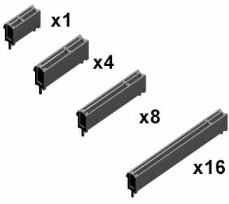
PCIe slots come in the following standard form factors.
PCI Express x1 slot
PCI Express x4 slot
PCI Express x8 slot
PCI Express x16 slot
Credit Erwin Mulialim / Wikimedia Commons / CC BY-SA 3.0
These are classified purely by the physical size of the slot.
Some PCI Express slots have the physical form of a PCI Express x16 slot
but internally support only x8 lane bandwidth.
Likewise, a PCIe expansion card may have a physical x16 form factor
but only use x8 lane bandwidth.
Remember that the slot form factor and the number of lanes actually used internally do not necessarily match.
Number of PCI Slots
For E-ATX and ATX form factors (cases), the number of PCI Express slots is 7.
That's all for this installment.
Thank you for reading.
Next time, I would like to deepen our understanding by looking at the block diagram of an actual chipset.
Looking beyond DIY builds toward GPU environments for research and business?
The know-how gained from building your own GPU machine carries over directly to infrastructure choices for research, PoCs, and production.
We build and operate our own GPU cluster in-house and develop LLM products on it. We can also support a wide range of needs, from procuring GPU workstations for research to Intel Core and Intel Xeon architectures, covering everything from consumer to professional use. Beyond helping you procure and build workstations, we advise on what comes next, from setting up training environments to selecting the right GPUs, optimizing inference, and designing distributed configurations, all based on hands-on operational experience.
See our LLM infrastructure and platform technology services →navigation